KAHKEE Mall

Fully Vacuum Interconnected MoCVD/MBE Integrated Equipment

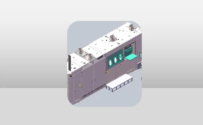
This domestically produced high-end semiconductor material growth equipment, benchmarked against AIXTRON’s core technology, is designed specifically for compound semiconductor R&D and mass production. It supports vacuum interconnection between MoCVD and MBE systems, enabling contamination-free and efficient substrate transfer, meeting the needs of both scientific research and industry.

It is used in industrial fields, mass production of high-power LED chip epitaxial radio frequency devices (HEMT), photovoltaic thin-film battery deposition and other fields.

Learn more
Technical Specifications
Epitaxial Equipment Performance
 Single furnace capacity Optional: 19X2”, 15X4”, 8X6”, 5X8”
 Substrate types Sapphire (GaAs), Gallium Phosphide (GaP), Indium Phosphide (InP), Silicon (Si), Silicon Carbide (SiC), Gallium Nitride (GaN)
Epitaxial growth specifications Growth rate: 1-4µm/hour
Temperature uniformity <±3℃(at 1000°C)
Temperature control range 100~1200℃
Heating rate 0.5℃-3℃/s, continuously adjustable
Pressure control range 20-760 Torr, continuously adjustable, accuracy: 3 Torr
Reaction chamber design Made of high-quality, high-temperature and corrosion-resistant materials
Substrate rotation speed 0-1500, continuously adjustable
Vacuum tightness Piping system leakage rate: <1×10⁻⁹ Pa·L/S
Reaction chamber leakage rate: <3×10⁻⁹ Pa·L/S


Key Technological Breakthroughs
Vacuum interconnect technology A proprietary transition chamber design enables full-process vacuum integration between MoCVD and MBE systems, preventing oxidation contamination to substrate
Dual-zone reaction chamber Independent temperature control modules supports process switching for GaN, Ga₂O₃, and 2D materials, improving R&D efficiency by 40%
Industrial-grade reliability Modular design ensures >8,000 hours of trouble-free operation throughout the year, with a mass production yield of ≥99.5%
Other Products

欢迎咨询

我们将在收到询盘后24小时内回复您,并根据您的咨询内容提供专业解决方案。